

Take a look at the essential concepts, terms, quotes, or phenomena every day and brush up your knowledge. Here’s your knowledge nugget on the key technology of semiconductors for today.
India’s semiconductor ambition received a major boost when Prime Minister Narendra Modi visited the Netherlands for an official visit on 16-17 May 2026. During the visit, PM Modi and the Prime Minister of the Netherlands, Rob Jetten, signed 17 pacts spanning semiconductors, critical minerals, migration, water management, and renewable energy.
1. As part of a major push for semiconductors, a Memorandum of Understanding for semiconductors was signed between Tata Electronics and ASML to support the establishment and ramp-up of its upcoming 300 mm (12-inch) semiconductor fabrication plant in Dholera, marking a giant step in India’s semiconductor manufacturing ambitions.
2. Why is ASML strategically important? ASML is the world’s only producer of extreme ultraviolet (EUV) lithography machines, the highly sophisticated systems required to manufacture advanced semiconductors. Without its machines, the production of cutting-edge chips becomes virtually impossible.
3. According to ASML, EUV lithography prints microchips using light with a wavelength of just 13.5 nm – almost x-ray range. Lithography, more formally known as ‘photolithography’, is a projection system. Light is projected through a blueprint of the pattern that will be printed (known as a ‘mask’ or ‘reticle’).
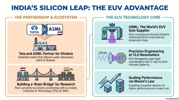 Created using Notebooklm
4. The pattern is encoded in the light, which allows the system’s optics to shrink and focus the pattern onto a photosensitive silicon wafer. After the pattern is printed, the system moves the wafer slightly and makes another copy on the wafer.
5. EUV is driving Moore’s Law forward and supporting novel transistor designs and chip architectures. In 1965, Intel co-founder Gordon Moore observed that the number of transistors on a microchip was increasing rapidly.
Story continues below this ad
6. He predicted that the number of transistors in a microchip would double every year for the next decade which he revised to every two years in 1975. His prediction is known as Moore’s Law.
7. Moore’s Law is not a natural law as we know in physics and chemistry but it has a huge impact on the speed of technology. Today by repeatedly doubling the number of transistors on a chip, chipmakers are delivering higher performance at lower cost with each new generation of chip.
8. To enable this, chipmakers are relying more and more on exotic materials, advanced packaging technologies and more complex 3D transistor designs to deliver improved chip performance. That’s where EUV lithography comes in. It makes scaling more affordable for chipmakers and allows the semiconductor industry to continue its pursuit of Moore’s Law.
What were the major outcomes of the India-Netherlands meeting?
1. India and the Netherlands have decided to elevate their bilateral ties to a ‘Strategic Partnership’ by agreeing on a comprehensive five-year roadmap (2026–30).
Story continues below this ad
2. Both the countries have established a “brain bridge” in semiconductor research through a Memorandum of Cooperation between the Eindhoven University of Technology, the University of Twente, and six premier Indian institutes: IISc Bangalore, IIT Bombay, IIT Delhi, IIT Gandhinagar, IIT Guwahati, and IIT Madras.
3. On defence cooperation, they agreed to plan a structured Joint Tri-services interaction between the Ministries of Defence and the Directorates of International Military Cooperation to coordinate bilateral military cooperation, including cooperation between Defence Industry and Research Centres
4. On the migration pact, the statement said they agreed to strengthen cooperation to prevent and combat irregular migration and trafficking in human beings, and to encourage the fair mobility of highly skilled professionals.
BEYOND THE NUGGET: GaN (Gallium Nitride) technology
1. Earlier this month, the Union Cabinet approved two new semiconductor plants in India, including one that could be the country’s first display fabrication facility. With these, the government has approved a total of 12 chip plants under the first leg of the India Semiconductor Mission (ISM) in states like Gujarat, Assam, Andhra Pradesh, Uttar Pradesh, and Odisha.
2. The approval is given to a Rs 3,068 crore compound semiconductor fabrication and assembly based on GaN (Gallium Nitride) technology for manufacturing Mini/Micro-LED display modules to be set up by Crystal Matrix Ltd.
3. Semiconductors are made of materials such as silicon and possess a degree of electrical conductivity between that of a conductor and an insulator. Silicon has been the component mostly used in semiconductors.
4. In recent years, gallium nitride (GaN), another semiconductor, has been making its way into electronics as it is better suited for high-power and high-frequency applications.
Story continues below this ad
5. Gallium Nitride is a material that is considered a better alternative to silicon. It is much better at conducting high voltage over longer times compared to silicon. It also allows electric current to flow faster through it.
6. With lower heat, Gallium Nitride structures can be stacked closer to each other than other materials, which also means the overall structure (the charger) is smaller in size.
| Semiconductor Plant | Location |
| Tata Electronics semiconductor foundry | Gujarat |
| Micron Technology | Gujarat |
| Kaynes Semicon | Gujarat |
| CG Semi | Gujarat |
| Crystal Matrix | Gujarat |
| Suchi Semicon | Gujarat |
| Tata Electronics assembly unit | Assam |
| HCL-Foxconn | Uttar Pradesh |
| SiCSem | Odisha |
| 3D Glass Solutions | Odisha |
| Advanced System in Package Technologies | Andhra Pradesh |
| Continental Device | Punjab |
Post Read Question
Which one of the following pairs of semiconductor plants in India and their locations is not correctly matched? (UPSC CSE 2026)
Story continues below this ad
(a) CG Power and Industrial Solutions Pvt. Ltd. in partnership with Renesas Electronics and STARS Microelectronics: Gujarat
(b) Tata Semiconductor Assembly and Test Pvt. Ltd.: Assam
(c) HCL-Foxconn Joint Venture India Chip Ltd.: Madhya Pradesh
(d) SicSem Pvt. Ltd.: Odisha
(Sources: India, Netherlands seal historic 17-pact strategic partnership on chips, defence, 12 semiconductor plants approved, ASML, ISM)
Subscribe to our UPSC newsletter. Stay updated with the latest UPSC articles by joining our Telegram channel – IndianExpress UPSC Hub, and follow us on Instagram and X.
🚨 Click Here to read the UPSC Essentials magazine for May 2026. Share your views and suggestions in the comment box or at manas.srivastava@indianexpress.com🚨